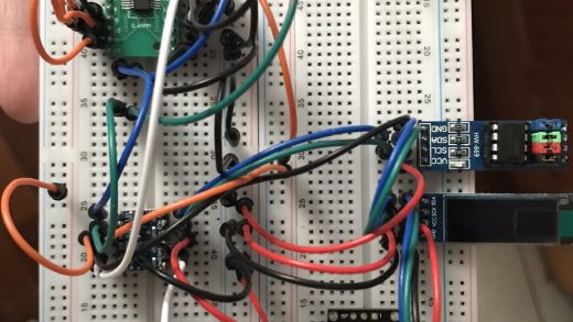
While learning AD24 recently, I discovered an issue:
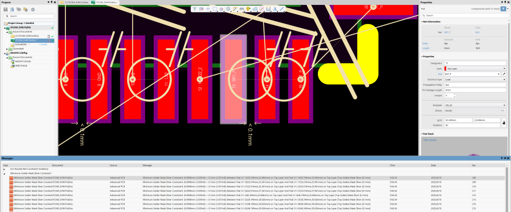
As shown in the screenshot, AD’s DRC check reported a violation:
“[Minimum Solder Mask Sliver Constraint Violation] IP2369_EVM.PcbDoc Advanced PCB Minimum Solder Mask Sliver Constraint: (0.0998mm (3.929mil) < 0.1mm (3.937mil)) Between Pad U1-21 (52.014mm, 25.561mm) on Top Layer And Pad U1-22 (52.014mm, 25.961mm) on Top Layer [Top Solder] Mask Sliver [0.1mm]”
After investigating and manually calculating pad size, solder mask expansion, and pad spacing:
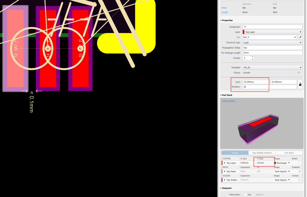
For the two pads at the violation threshold, the left X is 50.349mm and the right X is 50.749mm. Pad center spacing is 0.4mm, pad width is 0.2mm, and solder mask expansion follows the rule set to 0.05mm (SolderMaskExpansion). These parameters follow JLCPCB’s manufacturing specs, and the footprint was imported from JLC EDA. The solder mask bridge spacing also follows JLC’s guideline article: 技术指导:阻焊基本设计, which recommends 0.1mm. Based on these parameters, manual calculation gives: 0.4mm – 2 x 0.1mm – 2 x 0.05mm = 0.1mm This does not violate the DRC rule of < 0.1mm. But AD reports the spacing as 0.0998mm.
After searching online, I found someone mentioning floating point standard issues (link lost, but the symptoms were similar). This made me suspect floating point precision. I then tried changing the DRC rule Minimum Solder Mask Sliver Constraint to 0.099. Running DRC again, the error disappeared.
Not sure if this introduces any risk, but for now it removes the annoying warnings.
博主友情提示:
如您在评论中需要提及如QQ号、电子邮件地址或其他隐私敏感信息,欢迎使用>>博主专用加密工具v3<<处理后发布,原文只有博主可以看到。