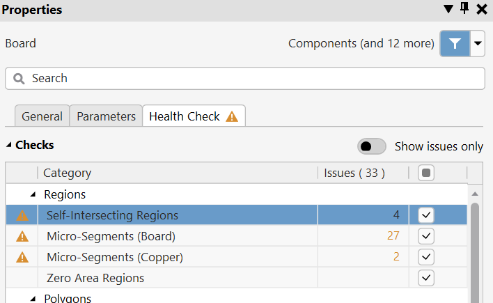
As shown in the screenshot, while learning PCB design in AD recently, I discovered that besides DRC checks, AD also has a Health Check feature (the version used when writing this was 25.8.1). Several warnings appeared: Self-Intersecting Regions、Micro-Segments (Board)、Micro-Segments (Copper). This record mainly focuses on a strange issue encountered while fixing the first and third problems.
First, by clicking the issues listed:
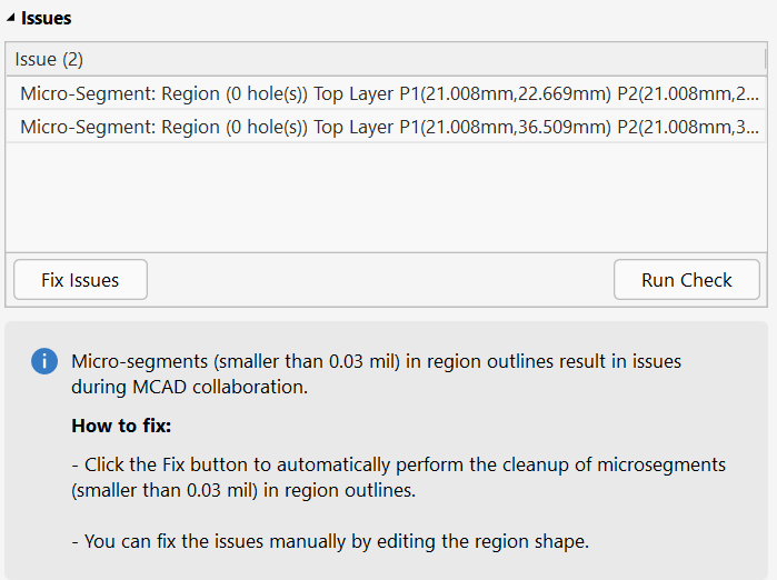
You can locate the PCB area where the problem was detected. In my board, it pointed to this location:

I saw that it was a MOSFET. Based on the issue description, it seemed like the footprint contained some very small fragments that might cause manufacturing problems. But honestly, I could not visually identify the issue. For these types of issues, AD allows manual fixing or using the Fix button. I clicked Fix, the issue disappeared, and nothing visibly changed on the PCB. Then I checked the first issue:
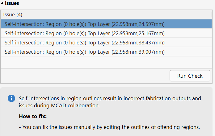
This Self-Intersection issue also pointed to the MOSFET footprint, but this time there was no one-click fix. It had to be repaired manually. I wondered whether the MOSFET footprint had some nonstandard geometry (note: I did not draw this footprint myself; the schematic symbol, footprint, and 3D model were all imported from JLCEDA via Weida). So, with the intention of understanding the root cause, I reverted the previous fix and decided to investigate both issues together. Clearly, the problem had to be inside this MOSFET footprint.
Opening the footprint in the component library and checking the layers mentioned in the Health Check report, I finally found the issue:
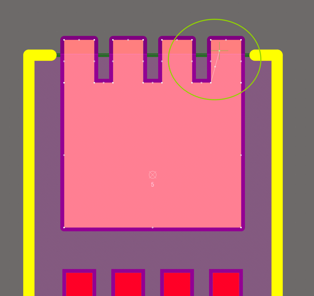
One of the pads had an extra line segment. I was not sure whether this was caused by JLCEDA import or an error in the original footprint drawing. I removed the extra geometry, saved, recompiled the library, exported the integrated library, and then tried updating the PCB component. And then something strange happened:
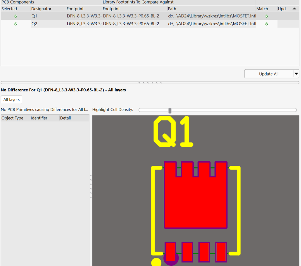
AD did not detect any footprint changes and refused to update. I confirmed multiple times that the modified library was indeed recompiled, and the file timestamps had changed. But AD still insisted that the footprint had not changed.
Thinking about it, I suspected that AD’s matching logic might ignore changes that do not affect pad geometry. From the pad’s final shape, the modification indeed did not change the pad outline. So I intentionally modified the pad incorrectly:
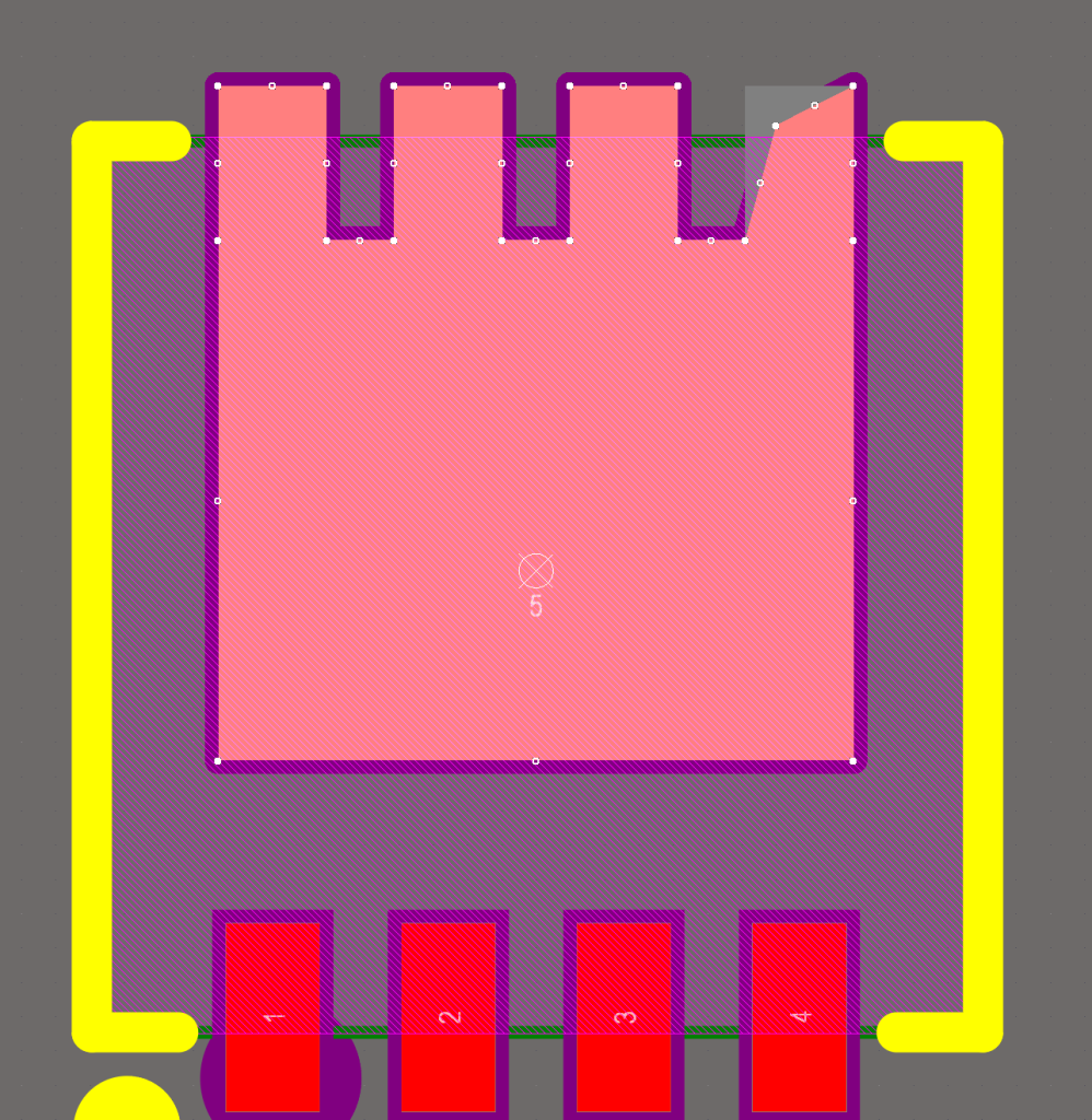
After saving, compiling, exporting, and updating the PCB component again, this time AD detected the mismatch:
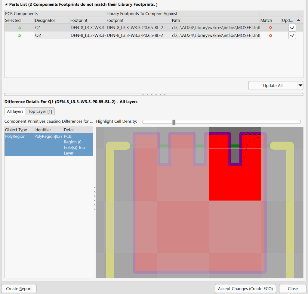
The Match column showed a red cross. This confirmed my suspicion about how AD determines footprint changes. I applied the incorrect modification, then returned to the library, reverted the footprint to the correct version, recompiled, and updated the PCB again. This time AD detected another mismatch, and after updating, the footprint was finally corrected.
Then, the Health Check showed that the results were outdated:
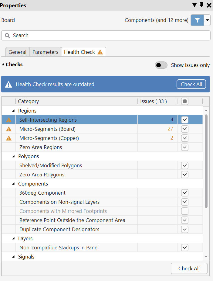
After clicking Check All to refresh, all issues under the three categories disappeared.
博主友情提示:
如您在评论中需要提及如QQ号、电子邮件地址或其他隐私敏感信息,欢迎使用>>博主专用加密工具v3<<处理后发布,原文只有博主可以看到。